Overview: What is a computer?
At a high level, any computer can be viewed as consisting of the
following abstract components:
Input
Output
Memory
Processor = (Datapath + Control)
The processor can be viewed as consisting of two distinct
sub-components: Datapath is the hardware responsible for
performing all required operations (e.g. ALU, registers, internal
buses), and Control is the hardware that tells the datapath
what to do e.g. in terms of switching, operation selection, data
movement between ALU components, etc. (Patterson and
Hennessy 2011).
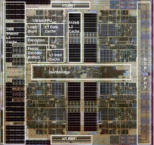
As a concrete example, below is a photograph of the quad-core AMD
Barcelona processor chip, originally shipped in 2007, with overlaid
diagram describing the various subcomponents.
The
Processor
To understand the basics of a processor implementation, we can look
at the construction of the datapath and control path for an
implementation of the MIPS instruction
set. This includes a subset of the core MIPS instruction set:
The memory reference instructions load word (lw) and
store word (sw)
The arithmetic-logical instructions
add,sub,AND,OR, and
slt
The instructions branch equal (beq) and
jump(j)
Overall, much of what needs to be done to implement these
instructions is the same regardless of the exact class of instruction.
For every instruction, the first two steps are identical:
Send the program counter (PC) to the memory that contains the
code and fetch the instruction from that memory.
Read one or two registers, using fields of the instruction to
select the registers to read.
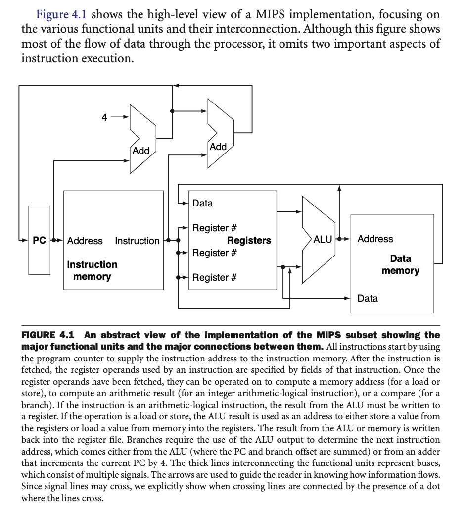
For example, the diagram below shows a high level, abstract outline
of a MIPS processor implementation.

Logic Design Conventions
Note that the datapath elements of a MIPS implementation consists of
two different type of logic elements:
Combinational: elements that operate on data
values, where their outputs always depend only on the current inputs
(i.e. think of them as implementing pure functions)
Sequential: elements that contain some internal
state. These elements have at least two inputs and one output,
where the inputs are:
The data value to be written.
The clock.
The output from a sequential logic component provides the value that
was written in an earlier clock cycle.
A clocking methodology defines when signals can be read and
when they can be written. We can assume an edge-triggered
clocking methodology, which means that any values stored in a
sequential logic element are updated only on a clock edge.
Since state (i.e. sequential) elements are the only ones that can
store values, any collection of combinational logic must have its inputs
come from a set of state elements and its outputs written into a set of
state elements The inputs are values that were written in a previous
clock cycle, while the outputs are values that can be used in a
following clock cycle.
Pipelining
MIPS instruction execution classically takes five steps:
Fetch instruction from memory.
Read registers while decoding
the instruction.
Execute the operation to calculate an
address.
Access an operand in data memory.
Write the result into a register.
The
Memory Hierarchy
In an ideal world, we would have an infinitely large and fast memory
for our computer, but this is not feasible in practice, since fast
memory is costly. So, instead, we simulate the illusion of an infinite
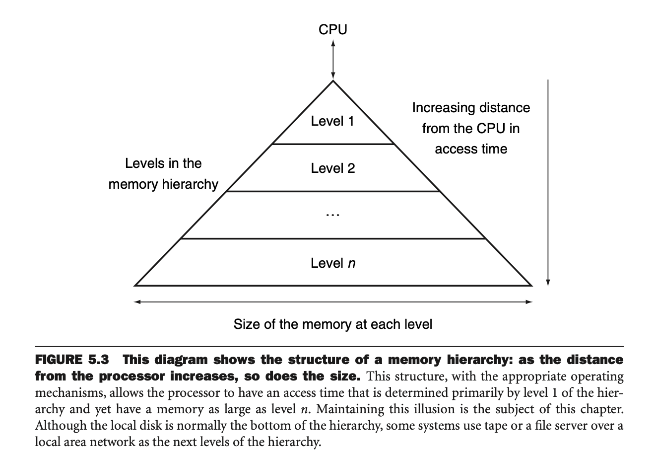
memory by using a memory hierarchy. That is, a progressively
larger and slower series of caches that serve as memory for the
processor.
Note that the principle of locality underlies the way that
programs operate. That is, the assumption is that programs access a
relatively small portion of their address space at any instant of time.
There are two different types of locality:
Temporal locality: if an item is referenced at
some point in time, it is likely to be referenced again soon.
Spatial locality: if an item is referenced,
other items that are nearby are likely to be referenced soon.
We make use of this to construct the memory hierarchy from a series
of caches, that get progressively faster and smaller as they
get closer to the actual processor.
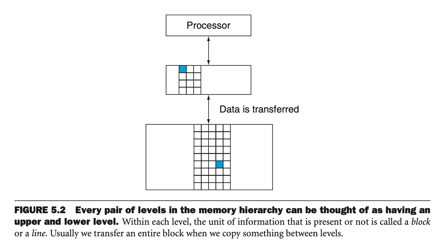
A memory hierarchy may consist of multiple levels, but data is copied
only between two adjacent levels at a time, so we can consider only two
levels when describing the caching mechanisms. There is an upper
level (faster and closer to the processor) and a lower
level. The smallest unit of information that can be either present
or absent from any cache level is typically referred to as a cache
block or line.

Cache Basics
In a basic scenario, we can imagine that a processor issues memory
requests that are each one word (e.g. 32 bits) and the blocks in the
cache are also one word. If a cache contains words \(X_1,\dots,X_{n-1}\) prior to a request for
a word \(X_n\) not in the cache, then a
cache miss occurs and \(X_n\) is
brought into the cache.
When servicing a processor request, we need to know (1) is the data
item in the cache and, if so, (2) how do we find it? The simplest
approach is to simply map each word to a locatino in the cache based on
its address, which is known as direct mapping. This is
essentially a simple hash based addressing scheme. With this approach,
however, there may be collisions in addresses that map to the same cache
location, so we need to deal with this. One approach is to add a set of
tags to the cache. Basically, for each cache entry, we add a
tag that contains the bits of the address that were not included in the
hash function, so that we can disambiguate between two addresses that
may map to the same cache location. In practice we may also include a
valid bit that tells whether a particular cached value is
currently valid to use or not.
Set Associative Caches
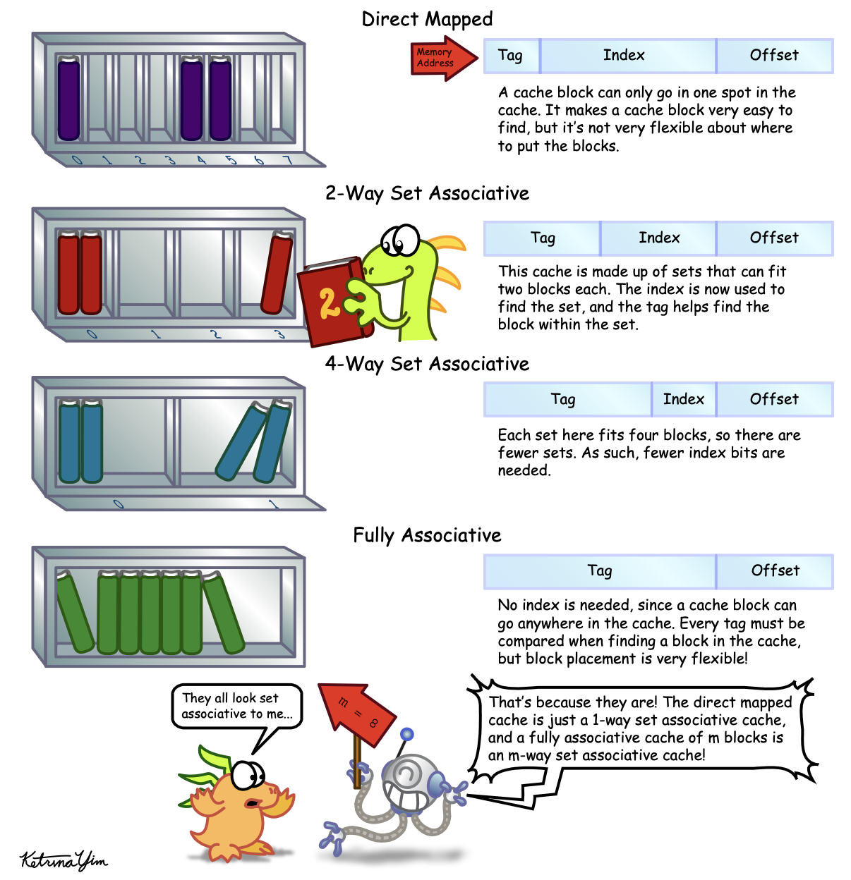
An alternative to the direct mapping approach is to make the cache
set associative. So, instead of giving every address exactly
one location in the cache, we give it \(n\) possible locations, which we call \(n\)-way set associative. If the cache can
hold \(m\) entries then a \(m\)-way set associative cache is also
referred to as fully associative. In this other extreme, it
means that a block can be placed anywhere in the cache, but then comes
with the tradeoff that finding a block is more expensive, since we may
need to search through every block to find it.

Note that allowing for more potential locations for a block can
decrease contention for blocks, since if there are only a few unused
blocks, a new request is then free to pick any unused block. This is in
contrast to a direct mapped scheme, where choice of block is completely
determined by the address mapping function. Also, in an associative
cache, we have a choice of where to place the new block, so potentially
a choice of which block to kick out of the cache. The most commonly used
scheme is least recently used (LRU) i.e. we remove blocks that
were unused for the longest time.
Parallelism and Memory: Cache Coherence
For multicore processors, multiple processors likely operate on a
common physical address space. If different processors have their own
caches, though, then this means that the view of memory held by
different processors may be mismatched i.e. two processors see different
values for a given memory location. This issue is generally referred to
as the cache coherence problem.
Informally, we might want to define a memory system as being coherent
if any read of a data item returns the most recently written value of
that data item. This is a bit too simplistic, though, and this
definition contains two different aspects of memory system behavior. The
first, coherence, defines what values can be returned
by a read. The second, called consistency, determines
when a written value will be returned by a read. Considering
coherence first, we say that a memory system is coherent if
A read by processor \(P\) to a
location \(X\) that follows a write by
\(P\) to \(X\), with no writes of \(X\) by another processor occurring between
the write and the read by \(P\), always
returns the value written by \(P\).
A read by a processor \(P_1\) to
a location \(X\) that follows a write
by another processor \(P_2\) to \(X\) returns the value written by \(P_2\) if the read and write are
“sufficiently separated" in time and no other writes to \(X\) occurred between the two
accesses.
Writes to the same location are serialized. That is, two
writes to the same location by any two processors are seen in the same
order by all processors.
The first property establishes a basic local ordering property for
each processor i.e. it is what we would expect to hold true for a
uniprocessor system. The second property defines a notion of what it
means for multiple processors to have a coherent view of memory i.e.
processors should observe the most recent effects of writes by other
processors. The third property, write serialization, is also
required, to ensure that all processors observe writes to a particular
memory address in the same order.
Basic Schemes for Enforcing Coherence
In a cache coherent multiprocessor, the caches provide both
migration and replication of shared data items:
Migration: A data item can be moved to a local cache and
used there in a transparent fashion.
Replication: When shared data are being simultaneously
read, the caches make a copy of the data item in the local cache. This
reduces latency of access and contention for a read shared data
item.
The protocols to maintain coherence for multiple processors are
cache coherence protocols.
TODO: Snooping vs. directory-based cache coherence
protocols.
Virtual
Memory
In the same sense of smaller memory units acting as caches for main
memory, we can also view main memory as acting as a “cache” for external
storage: this technique is known virtual memory. The
motivations for virtual memory were historically twofold:
Eliminate the programming burdens of only having access to a
limited amount of main memory.
Allow safe and efficient sharing of memory between
multiple programs.
The latter is the more important consideration in modern systems
(since main memory units have gotten quite large). We would like to
compile programs such that they use their own address space
i.e. a separate range of memory locations accessible only to that
program. Virtual memory implements the translation of a program’s
address space to physical addresses.
Concepts between virtual memory and caches are essentially the same,
but things carry different naming conventions for historical
reasons.
With virtual memory, the processor produces a virtual
address, which is translated through a combo of hardware + software
into a physical address, which can be used to access main
memory. This process is called address translation. It’s just
another cache!
Making Address Translation Fast: the TLB
When a translation for a virtual page number is used, it will
probably be needed again in th near future. So, modern processors
include a special cache that keeps track of recent translations.
Typically this cache is called the translation-lookaside buffer
(TLB), but it would really be more appropriate to just call it a
translation cache.
Hardware Description Languages
Hardware description languages (HDLs) are languages for
describing digital circuits at a higher level of abstraction, rather
than directly describing every logic gate and their exact placement,
connections, etc.
Verilog
Verilog is one of the most common HDLs, and it can be used
to define both combinational and sequential circuits. As a simple
example, we can describe a simple combinational circuit in Verilog as a
module. For example, the following describes a circuit with one
input and one output, where the output is the negation
of the input.
    module top_module(input a, output b);
        assign b = !a;
    endmodule
When circuits become more complex, we can also declare
wires, which are like internal connections that are not
externally visible outside of the module. For example, the following
declares an internal wire that takes on the negation of the input
a, and this wire is then fed (i.e. connected to) the
output. For this simple example the wire doesn’t really serve a
necessary purpose, but with larger circuits wires can help to decompose
more complex bits of logic.
    module top_module(input a, output b);
        wire w1; // wire declaration.
        assign w1 = !a;
        assign b = w1;
    endmodule
Vectors
Vectors in Verilog are used to group related signals using one name
to make things more convenient. For example, declaring
wire [7:0] w; declares an 8-bit vector named w
that is functionally equivalent to having 8 separate writes.
Note how the declaration of a vector places the dimensions before the
name. But, note that the part select (i.e. accessing a
particular entry in the vector) has the dimensions after the
vector name e.g.
    wire [99:0] w; // declare 100 element vector.
    assign out = w[3]; // part select one bit of the vector.
More generally, the syntax for declaring vectors is as follows:
type [high:low] vector_name;
where type specifies the datatype of the vector
(typically wire or reg). Note that the
endianness of a vector is whether the least significant bit has
a lower index (little endian [3:0]) or a higher index (big
endian [0:3]). Once a vector is declared with a particular
endianness, it must always be used the same way.
